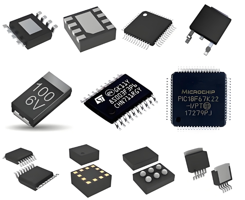
Lattice GAL16LV8C-15LJN: A Comprehensive Technical Overview of the 15ns High-Performance PLD
The Lattice GAL16LV8C-15LJN stands as a quintessential representation of high-speed programmable logic from a pivotal era in digital design. As a member of the widely adopted Generic Array Logic (GAL) family, this device combines the flexibility of programmability with impressive performance, encapsulated in a robust 20-pin PLCC package. Its designation, particularly the -15 suffix, directly indicates its maximum propagation delay of 15ns, positioning it as a high-performance solution for a vast array of logic integration applications.
Architecturally, the GAL16LV8C is built around a programmable AND array that feeds a fixed OR array, a structure known as a PAL®-like architecture. The device features 8 output logic macro cells (OLMCs), each of which can be individually configured by the user. This configurability is a key advantage, allowing each output to be programmed as a dedicated input, a registered output, or a combinatorial output with either active-high or active-low polarity. This versatility enabled designers to replace numerous standard fixed-function logic ICs with a single, unified GAL device, dramatically reducing board space, component count, and system cost.
A critical innovation of the GAL family, including the 16LV8C, was the use of Electrically Erasable (E2) CMOS technology. This technology was a significant leap forward from earlier fuse-based programmable devices. It allowed for ultra-low power consumption compared to bipolar alternatives and, most importantly, permitted the device to be reprogrammed and reused countless times. This reusability accelerated design iteration, prototyping, and field updates, fundamentally changing the development workflow for digital circuits.

The 15ns maximum propagation delay (tPD) is the defining feature of this specific variant. This speed grade ensured that the device could handle high-clock-frequency applications and was suitable for implementing critical timing functions like state machines, address decoders, and complex glue logic in microprocessor systems without becoming a bottleneck. The combination of high speed and low power made it ideal for performance-sensitive applications.
The integrated output registers are clocked by a dedicated clock pin, enabling the design of synchronous sequential circuits. Furthermore, a dedicated output enable pin provides tri-state control over all outputs, facilitating easy connection to bidirectional data buses. The device's 100% tested/100% routable architecture guaranteed that all timing parameters were met and that any valid design would fit without resource conflicts.
In summary, the Lattice GAL16LV8C-15LJN was a workhorse of programmable logic, offering a blend of speed, low power, and design flexibility that was unparalleled in its time. It served as a fundamental building block for consolidating and implementing complex combinatorial and sequential logic, paving the way for the more complex CPLDs and FPGAs that followed.
ICGOODFIND: The Lattice GAL16LV8C-15LJN is a high-performance, 15ns E2CMOS PLD featuring 8 reprogrammable macro cells. It excelled in logic integration for high-speed, low-power applications, reducing system cost and complexity.
Keywords: Programmable Logic Device (PLD), High-Speed (15ns), Electrically Erasable (E2) CMOS, Output Logic Macro Cell (OLMC), Low Power Consumption.
